Thin Film Photovoltaic Lab
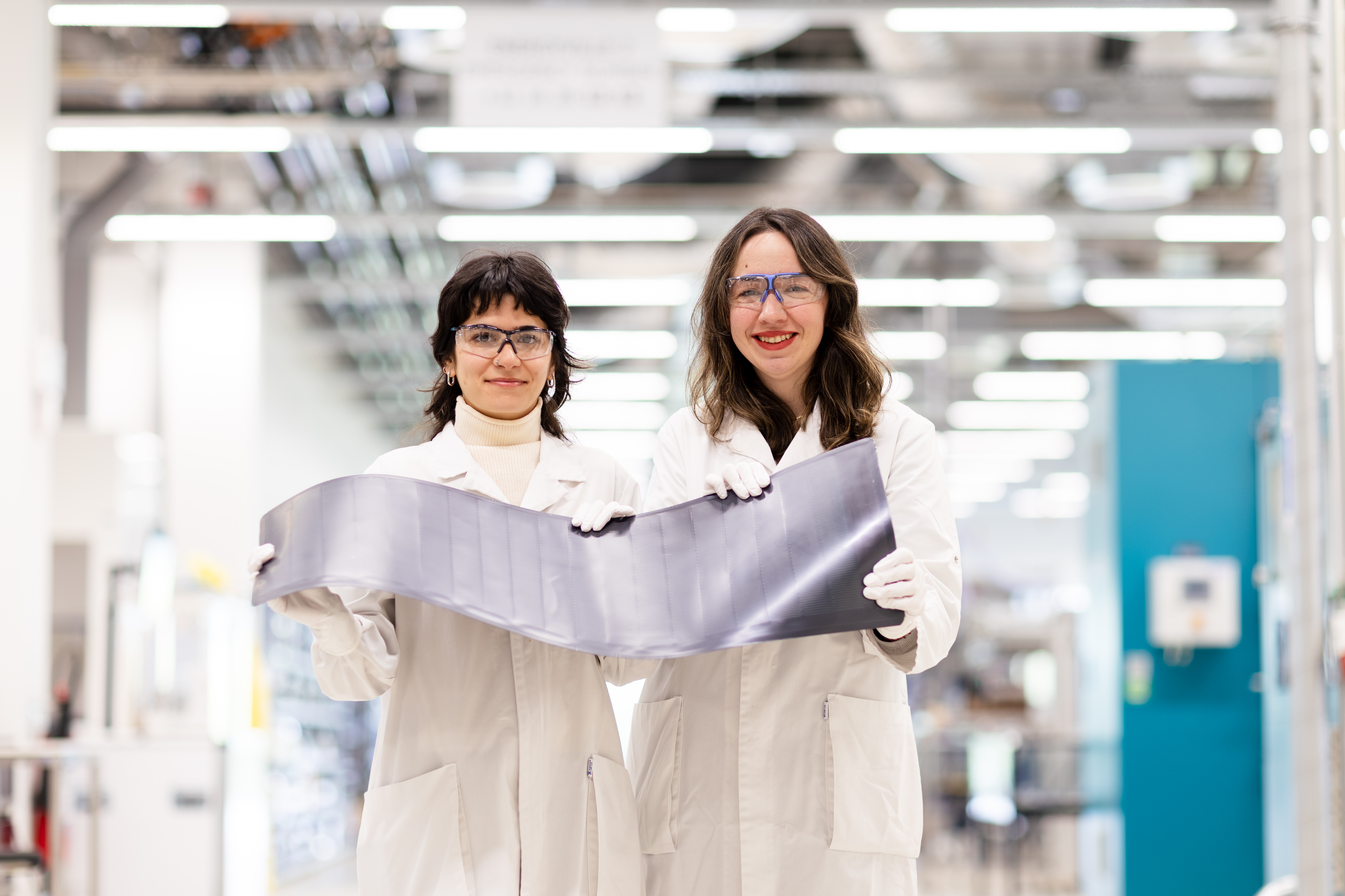
The field of photovoltaic energy is constantly evolving. New thin-film materials, such as perovskites and CIGS, are leading to solar cells with conversion efficiencies comparable to those of silicon cells, and all this at potentially lower costs and with more flexible dimensions.
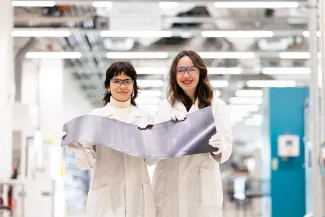
A thorough understanding of the properties of these new perovskite solar cells, in terms of both materials and device aspects, is essential for developing the processes that will enable the production of devices with the highest possible performance.
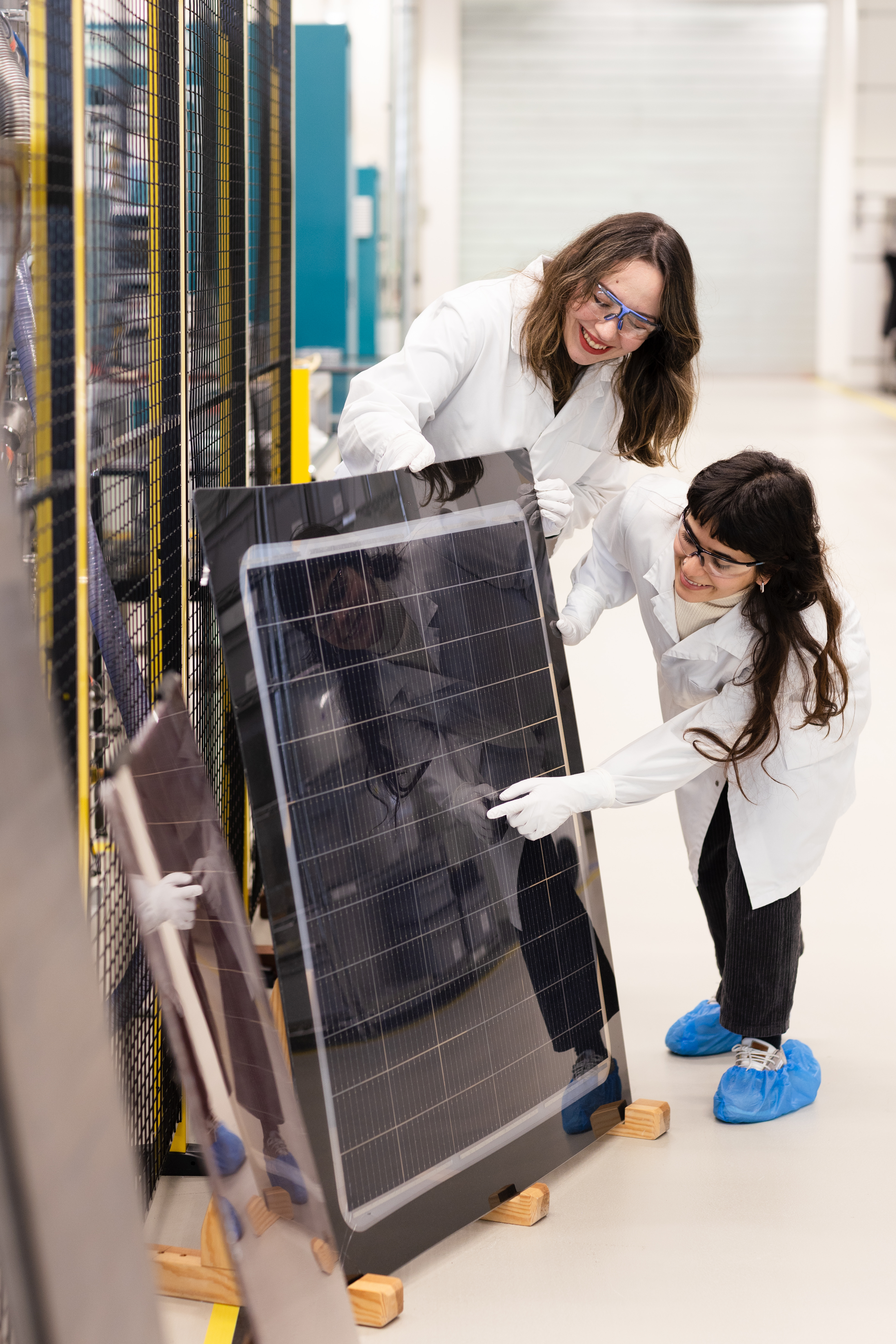
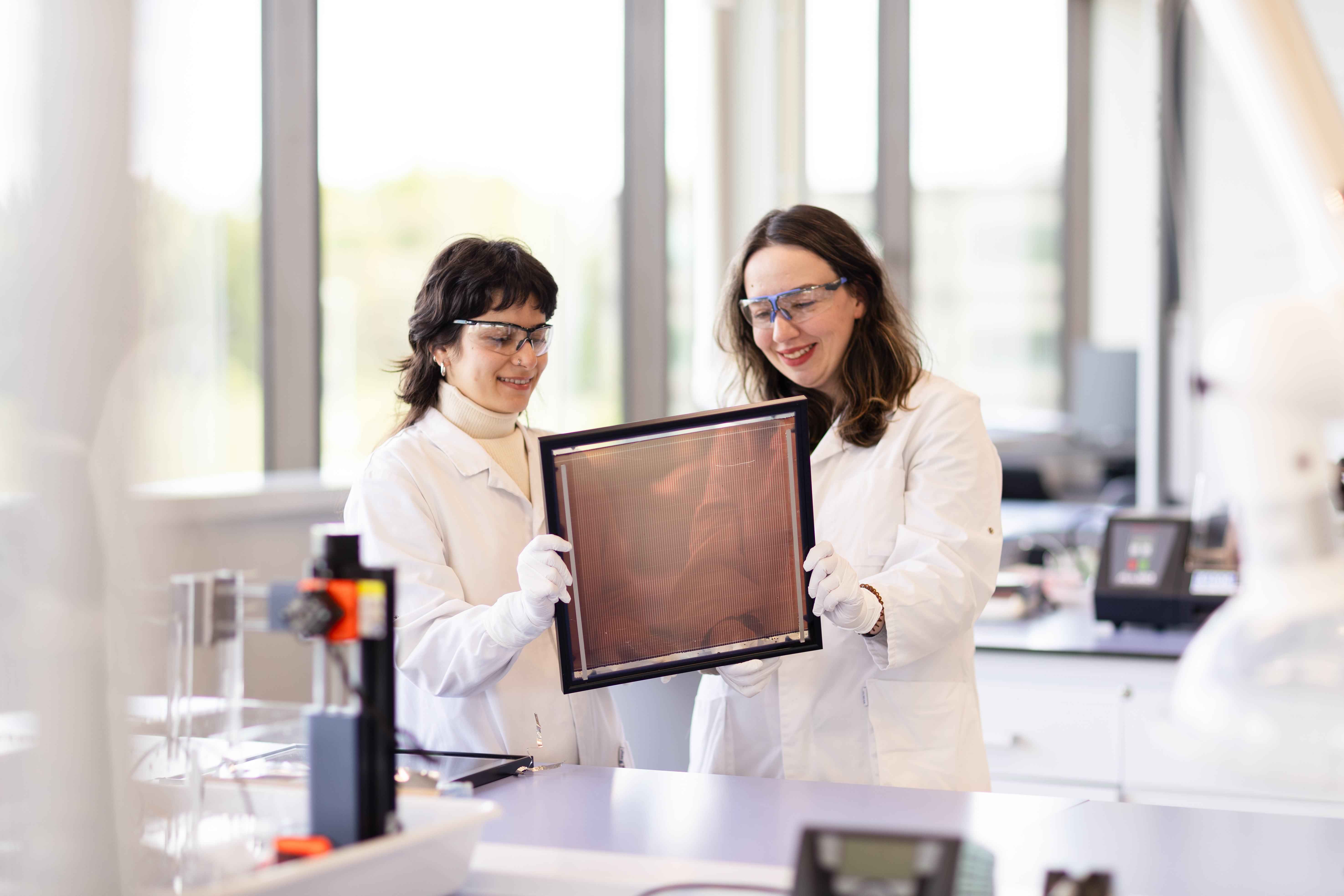
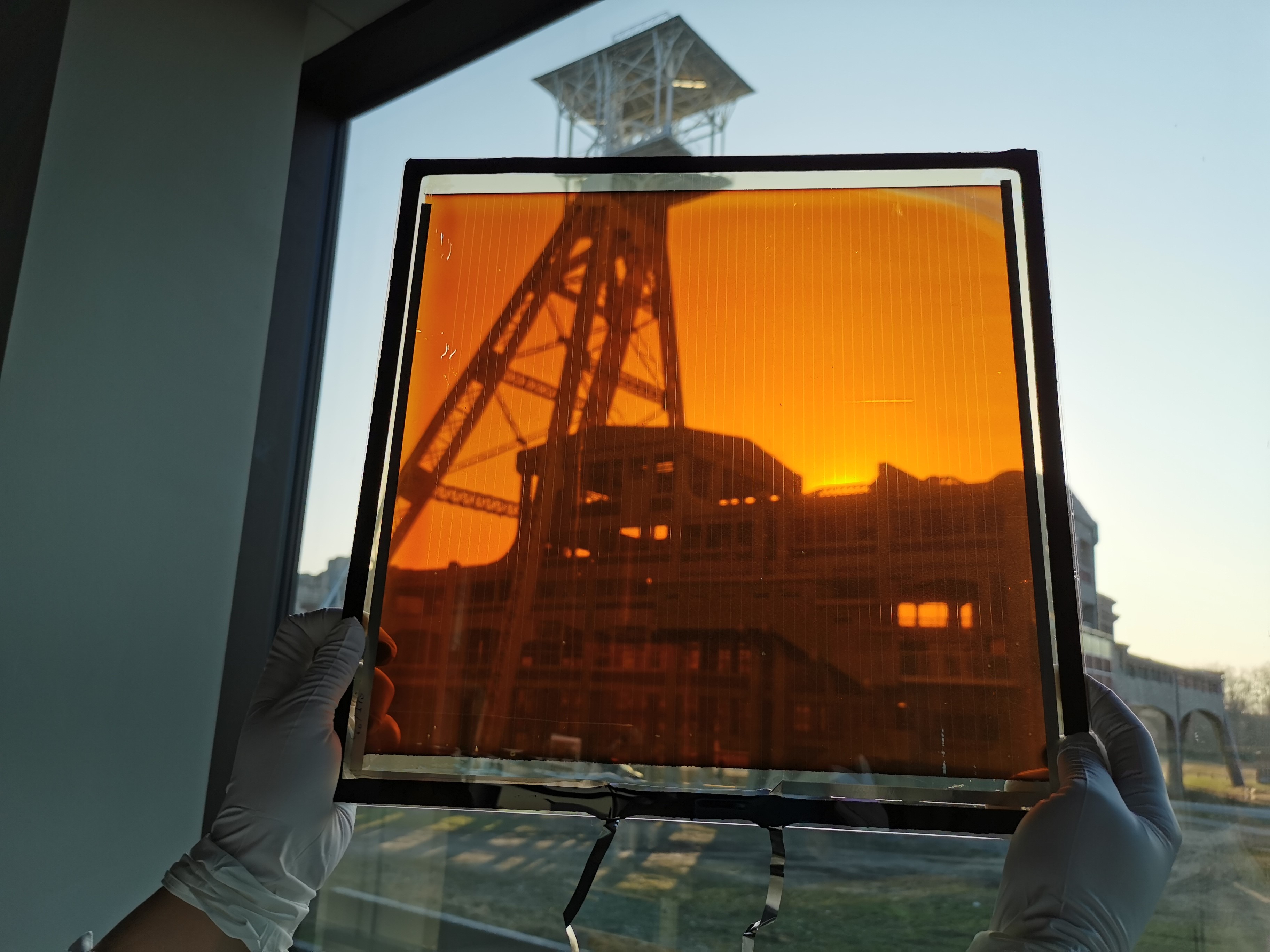
In the Thin Film Photovoltaic Lab, we demonstrate these new materials and device architectures, not only on small-scale laboratory devices but also on large-scale modules measuring 30×30 cm². Furthermore, we are taking this a step further by fully integrating this technology into end-use applications such as buildings, vehicles and infrastructure.
These thin-film PV technologies offer the possibility of combining with existing silicon solar cell technology in tandem solar cells. This synergy results in even higher conversion efficiency, enabling the current limitations hindering the further development of silicon photovoltaics to be overcome.
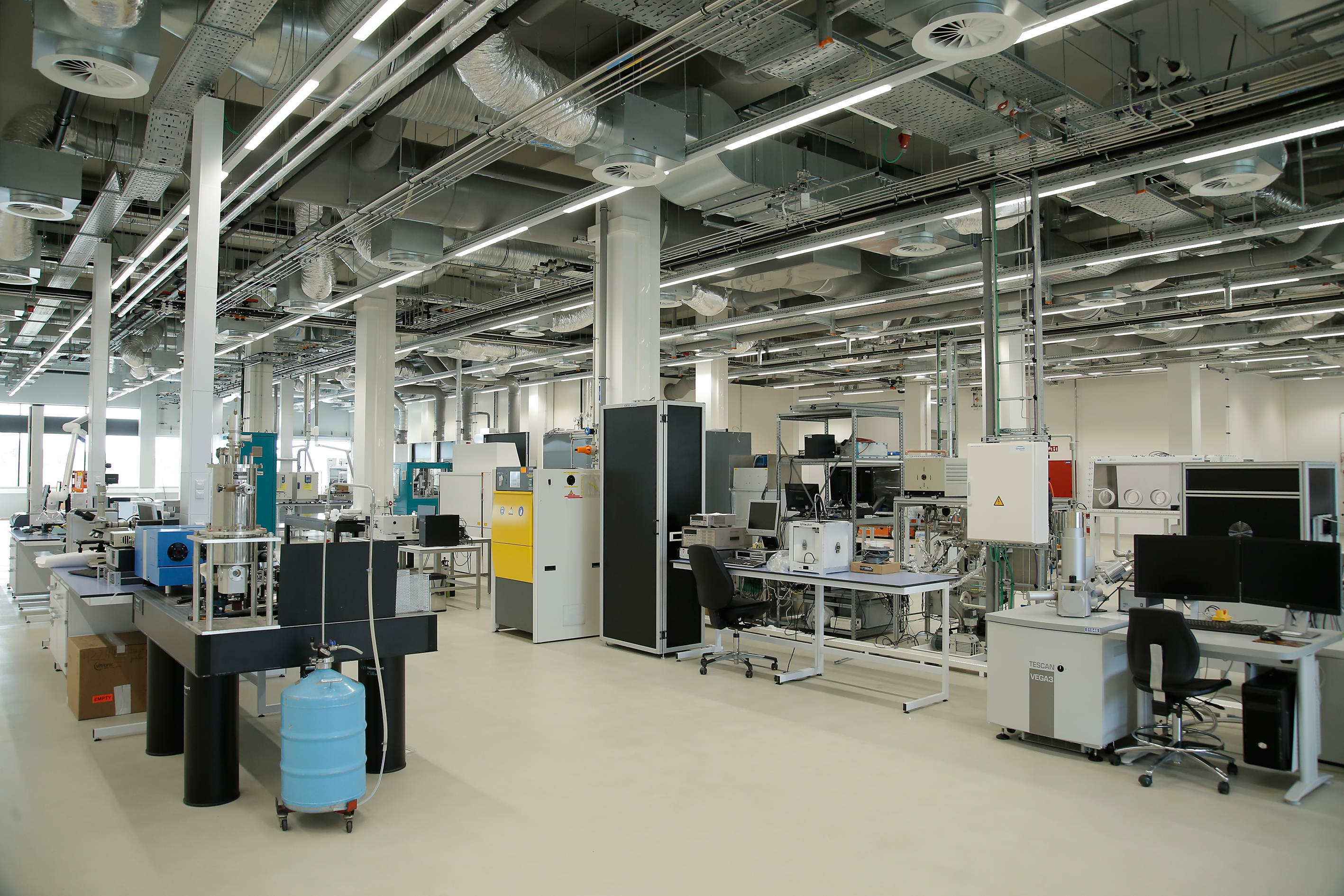
Take a tour of this lab
Take a look around our lab and discover how we conduct research into innovative energy solutions.
Who can use the Thin Film Photovoltaic Lab?
- Companies developing new thin-film photovoltaic materials.
- Manufacturers of module materials (encapsulants, sealants, glass, coatings).
- Developers and manufacturers of production technologies for thin-film deposition.
What is the purpose of the Thin Film Photovoltaic Lab?
- Joint projects on next-generation thin-film PV.
- Research into perovskites.
- Research into CIGS.
- Expertise in thin-film deposition.